This design is loosely based on the work of Xavier on the SMSPower forums, which I believe was a follow on
from Victor Kemp's work. I
jumped in at the tail end of this
forum topic and used all the information provided by the helpful people there to come
up with this design.
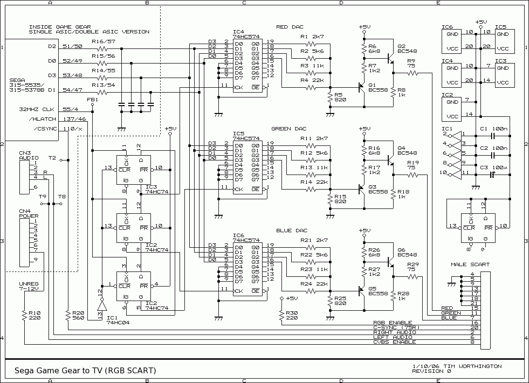
Sega's Game Gear is very similar in hardware to the their earlier game console, the
Master System. It is because of this legacy hardware that the internal LCD is driven with
TV compatible timing. This, and the availability of a composite sync signal on the PCB
(which seems to be there for this very reason, it's not used by any internal components!)
makes generating the video possible. The only problem is that the RGB data is sent
serially over four digital lines, one colour at a time. What my circuit does is separate
the red, green and blue video data using the signals provided from the board. I'm fairly
certain it works the same way as Sega's own development unit.
Three D flip-flops are used to divide the 32MHz master clock into three 5.3MHz pixel
clocks in a MOD-6 Johnson counter configuration. After every video line the counter is
reset by some kind of horizontal blanking pulse which goes to the LCD panel. I'm not
exactly sure what it's for but it does a very good job of synchronising the counter (once
it's inverted). I've named it /HLATCH on the circuit. The rising edge of each pixel clock
is used to latch the associated colour data in one of three octal D flip-flops (though
only half of each is used) and converted to analog with a binary weighted resistor ladder.
The analog video is then buffered by a 75 ohm driver stage before it goes to the
Television. /CSYNC is put through a resistor to get it to the correct voltage level for a
SCART video input, and both the RGB and CVBS status line are asserted to put the
destination TV in RGB video mode.
Download the circuit diagram and also the timing diagram to better understand how the pixel clocks are derived.
Download the Part Layout and Wiring Diagram and print it out
(it might be a good idea to trace the wires with coloured pens if you don't have a colour
printer). All parts required to build this circuit are
available from Jaycar Electronics. Their range
isn't very big so hopefully it should be easy for anyone to obtain the parts locally from
suppliers with a similar basic range.
I'm aware of two internally different versions of Game Gear. The newer and by far the
most common one is the single ASIC (Sega chip) version. The earlier version contains two
ASICs and more ram chips. Here are some photos to aid in locating various signals on the
board (though the circuit diagram should be sufficient for people who can read it). The
power rail (+5v and ground) can be picked off a nearby filter capacitor.
1asic_signal.png [91KB]
2asic_signal.png [141KB]
The circuit will be constructed on a piece of matrix style proto-board (not verroboard,
though the verro mob probably make it too). It's a phenolic board with a grid of 0.1"
holes punched and a single copper pad for each hole on the solder side. To fit all logic
ICs on the board we're going to take advantage of the fact that some of the ICs have many
pins connected in parallel, and stack them on top of each other. This method saves lots of
space and lots of wire. This is important because not only do we save many cents which
would have otherwise been wasted on board and wire, but we can also fit the circuit board
into the small empty void below the Game Gear's cartridge slot.
Here's a step-by-step (ok, more like jump-by-jump) pictorial guide to the construction and installation of the video amplifier/DAC board. This isn't intended to by a 'my first circuit' type of project - good soldering skills are required.
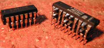
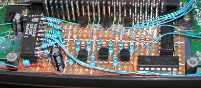
It's much easier to stack and solder the chips before they're on the board. Cut off unrequired outputs, join required inputs and bend out the pins on the 74HC374 first and second stories for the resistors. It's clear in this picture that I've forgotten to bend out the pin 11 clock input. On the left is the double stack of HC74s. Notice that I've connected the inputs of the unused half of the top chip to the inputs of the bottom chip, not +5v as shown on the circuit. I find it's easier this way, it doesn't really matter where they are connected as long as they are not left floating.
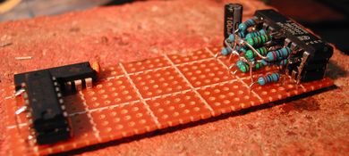
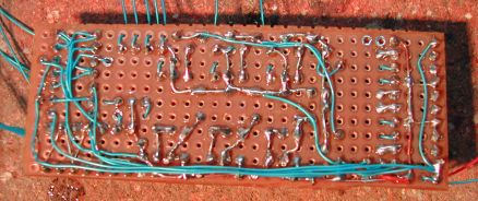
Chop up the proto-board into a piece 11 holes high and 30 holes wide. Solder the resistors onto the HC374 tower, stuff the rest of the ICs + bypass/filter capacitors on the board and we have something that looks like...
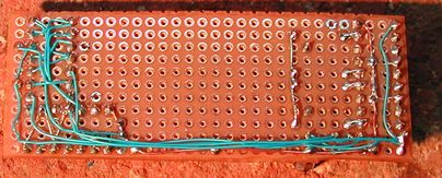
Now's the time to wire up the power supply lines to each chip. Once that's done all the logic wiring between the ICs needs to be taken care of. Keep the wires short and neat.
The final part, the video amplifier, is added in the middle. This connects to the isolated pads mid right in the picture above. Each input/output each need a wire soldered to it and poked up through an adjacent hole.
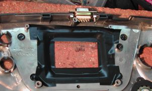
Use a file/cutters to cut a chunk out of the case above the screen for the 9 pin sub-D connector to be mounted. I recommend the female version because if you use a male connector one day some dope will plug a joystick into it and break something. When filing/drilling the case, place some tape around the edges of the screen opening to prevent plastic filings from getting trapped behind the plastic. Assign one of the pins on the sub-D as the 'ground' pin and solder a wire between it and the outer metal shell (or just wrap it around the screw).
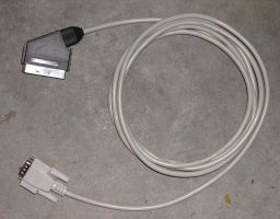
Next, make a DE9 -> SCART cable. If you have an RGB monitor you might want to substitute whatever it uses in place of the SCART. I built mine by cutting the end off a three meter long RS-232 (male on one end, female on the other) serial cable and attaching a male SCART connector. I find this works well but I do get a small bit of 60Hz hum in the audio from the video signal getting into the audio through signal cross talk. The only way to eliminate this would be to run the audio through a separate, shielded cable. A SCART pinout can be found here, decide on your own pinout for the D9 connector and write it down! Connecting the CVBS status line (SCART pin 8) is optional but may be required for some TVs to enter A/V mode.
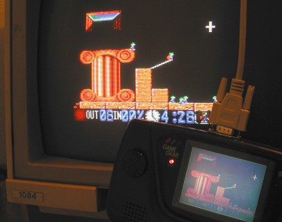
Blow out all the dust, put the guts back in and solder wires to the 9 pin D connector and to the various places on the main board. When everything is soldered in place (and all wires double checked) plug everything in, power it up, and see what happens. Hopefully the game (you put a game in, right?) is playing on the TV. The game gear has a lot of noise on its power supply rails. In my game gear this noise got into the video amplifiers and appeared as interference in the picture. To remove this I recommend putting an inductor in series with the +5v line that feeds our little board. This inductor should have 10µH or greater inductance and no more than an ohm or so of resistance. I used a 22µH RF choke.
When everything is tested and found to be working, place a strip of electrical tape
along the PC under the cartridge slot. Then place our modification board on top and hold
it in place with hot glue along the sides. If something goes wrong later the board can be
easily removed by cutting the hot glue.
SMS Power!
- The best internet resource for 8-bit sega console info.
 [
[